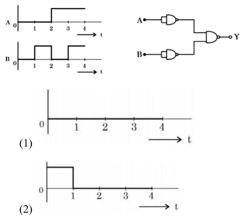
For the logic circuit shown, the output waveform at Y is:
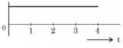
(A)(see structure)
(B)(see structure)
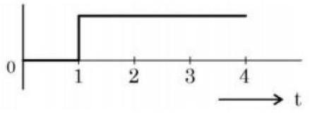
(C)(see structure)
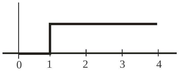
(D)(see structure)✓ Correct
Answer: (D)
Solution
Each input first passes through a NAND gate whose two inputs are tied together, so the upper gate produces A and the lower gate produces B. These two outputs feed the final NAND gate, giving Y=A⋅B=A+B, which is the OR operation. From the waveforms, A=0 for 0<t<2 and A=1 for 2<t<4, while B=1 only during 1<t<2 and 3<t<4. Applying Y=A+B: during 0<t<1 both inputs are low so Y=0; during 1<t<2 the input B is high so Y=1; and during 2<t<4 the input A is high so Y=1. Hence the output stays low from t=0 to t=1 and remains high from t=1 to t=4.
JEE Main · 2023 · 08 Apr 2023 · Shift 1 · Single correct option