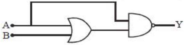
The truth table for the circuit given in the fig is :
(A)A0011B0101Y1000
(B)A0011B0101Y0011
(C)A0011B0101Y1111
(D)A0011B0101Y1100✓ Correct
Answer: (D)
Solution
Read the gate network in two stages. The OR gate combines the inputs into C=A+B, and the output stage is a NAND of A with that result, Y=A⋅C. Now test every input row. With A=0,B=0 we get C=0 and A⋅C=0, so Y=1. With A=0,B=1, C=1 but A⋅C=0, so Y=1. With A=1,B=0, C=1 and A⋅C=1, so Y=0. With A=1,B=1, C=1 and A⋅C=1, so Y=0. The output column is therefore 1,1,0,0.
JEE Main · 2019 · 12 Apr 2019 · Shift 1 · Single correct option