JEE Main · 2020 · 09 Jan 2020 · Shift 1 · Semiconductors

WhatsApp Email
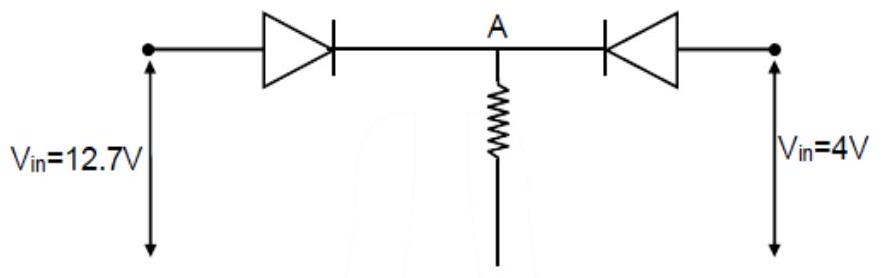
Both the diodes used in the circuit shown are assumed to be ideal and have negligible resistance when these are forward biased. Built in potential in each diode is 0.7 V. For the input voltages shown in the figure, the voltage (in Volts) at point is ____.

Answer: 12

Solution

The left diode has its anode held at V and the right diode has its cathode held at V, with point between them. The left diode conducts once V, and the right conducts once V. Because the higher source sits on the left, the left diode turns on and clamps the point while the right diode stays reverse biased. The voltage at is therefore V.

JEE Main · 2020 · 09 Jan 2020 · Shift 1 · Integer answer
More JEE Main questions on Semiconductors

  1. Find the correct combination of A, B, C and D inputs which can cause the LED to glow.
    JEE Main 2026View solution →
  2. For the given logic gate circuit, which of the following is the correct truth table?
    JEE Main 2026View solution →
  3. A voltage regulating circuit consisting of Zener diode, having break-down voltage of 10 V and maximum power dissipation of 0.4 W, is operated at 15 V. The approximate value of protective resistance in this circuit is ______ .
    JEE Main 2026View solution →
  4. Identify the correct truth table of the given logical circuit.
    JEE Main 2026View solution →
  5. Two p-n junction diodes and are connected as shown in figure. A and B are input signals and C is the output. The given circuit will function as a ______.
    JEE Main 2026View solution →
  6. The given circuit works as :
    JEE Main 2026View solution →