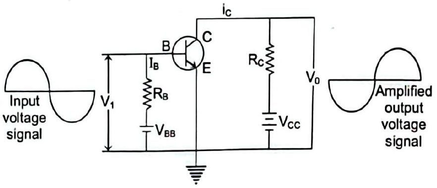
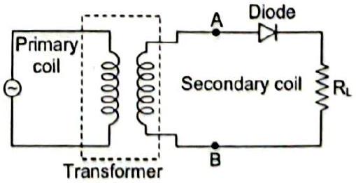
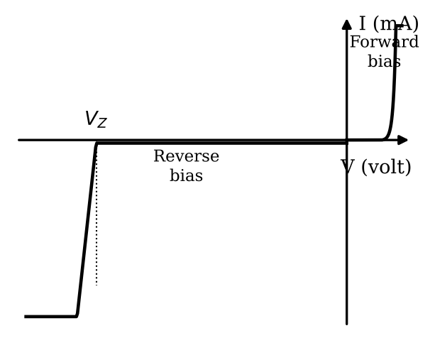
(i) Draw a circuit diagram to study the input and output characteristics of an n-p-n transistor in its common emitter configuration, and draw the typical input and output characteristics. (ii) Explain, with the help of a circuit diagram, the working of an n-p-n transistor as a common emitter amplifier.
Solution
(i) Connect the n-p-n transistor in CE configuration with VBB biasing the base (through a resistor) and VCC biasing the collector through RC, with meters for IB, VBE, IC, VCE. Input characteristic: IB versus VBE at fixed VCE. Output characteristic: IC versus VCE for several fixed IB. (ii) Amplifier: the base-emitter junction is forward biased and the collector-emitter output reverse biased through RC; the ac signal is applied to the base. The signal changes the base current, which produces a β-times larger change in collector current; the varying drop across RC is the amplified output, 180∘ out of phase with the input.