CBSE Class 12 · 2008 · SemiconductorsShort Answer

WhatsApp Email
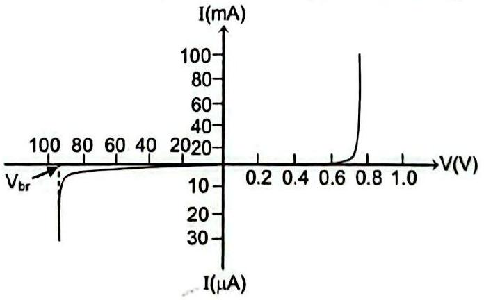
The figure shows the V-I characteristics of a semiconductor diode.
(i) Identify the semiconductor diode used.
(ii) Draw the circuit diagram to obtain the given characteristic of this device.
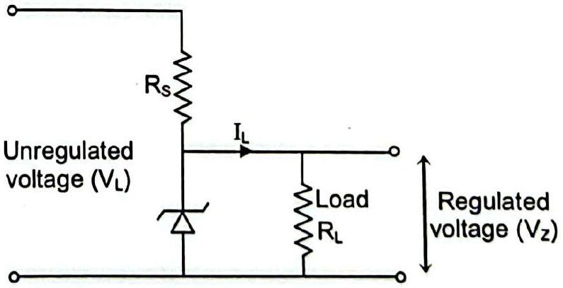
(iii) Briefly explain how this diode can be used as a voltage regulator.

Solution

(i) The characteristic shows a sharp reverse breakdown at a definite voltage, which identifies a zener diode.
(ii) To obtain it, connect the zener in reverse bias to a variable supply through a series resistance , with a voltmeter across the diode and a milliammeter in series.
(iii) Beyond the zener voltage the voltage across the diode remains essentially constant while the current changes greatly.
Connecting the load in parallel with the zener (with in series) keeps the load voltage fixed at despite supply or load changes — voltage regulation.

CBSE Class 12 Board · 2008 · Subjective

More board questions on Semiconductors

  1. A pure Si crystal having atoms is doped with 1 ppm concentration of antimony. If the concentration of holes in the doped crystal is found to be , the concentration (in ) of intrinsic charge carr …
    CBSE 2024View solution →
  2. (a) Explain the characteristics of a p-n junction diode that makes it suitable for its use as a rectifier.
    (b) With the help of a circuit diagram, explain the working of a full wave rectifier.
    CBSE 2024View solution →
  3. Explain the following, giving reasons.
    (a) A doped semiconductor is electrically neutral.
    (b) In a p-n junction under equilibrium, there is no net current.
    (c) In a diode, the reverse current is practically independent of the applied voltage.
    CBSE 2024View solution →
  4. In an extrinsic semiconductor, the number density of holes is . If the number density of intrinsic carriers is , the number density of electrons in it is
    CBSE 2023View solution →
  5. Pieces of copper and of silicon are initially at room temperature. Both are heated to temperature T. The conductivity of
    CBSE 2023View solution →
  6. The formation of depletion region in a p-n junction diode is due to
    CBSE 2023View solution →