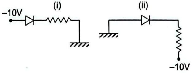
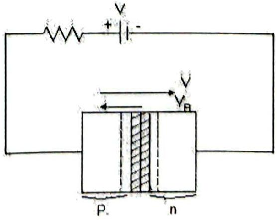
Explain, with the help of a circuit diagram, how the thickness of the depletion layer in a p-n junction diode changes when it is forward biased. In the following circuits, state which one of the two diodes is forward biased and which is reverse biased.
Solution
Forward bias connects the p-side to the positive and the n-side to the negative terminal, so the external field opposes the junction barrier field. Majority carriers are pushed towards the junction and neutralise some immobile ions, so the depletion layer becomes thinner and the barrier (VB−V) falls. For the two given circuits, the diode whose p-side is at the higher potential is forward biased: diode (ii) is forward biased and diode (i) is reverse biased. Forward bias thins the depletion layer; (ii) forward, (i) reverse.